





In the latest issue of SCIENCE CHINA Materials, Liu Jianping's team from Suzhou Institute of Nanotechnology and Nano-Bionics, Chinese Academy of Sciences published the research progress on GaN-based green laser diodes (LD).
The article uses various optical measurement methods to characterize the structure and chip of the green LD. (Article information: Tian, A., Hu, L., Li, X. et al. Greatly suppressed potential inhomogeneity and performance improvement of c-plane InGaN green laser diodes. Sci. China Mater. (2021). https:// doi.org/10.1007/s40843-021-1804-x)

(A) Device structure (b) Epitaxial structure
(C) Schematic diagram of the light distribution of the green LD perpendicular to the p-n junction
The characterization results show that when the excitation power density is 7 W cm-2, the photoluminescence half-height width at 300 K is 108 meV, and when the current density is 20 A cm-2, the electroluminescence half-height width is 114 meV. These The research results show that the uniformity of potential energy has been significantly improved. At the same time, the value of σ, which characterizes the distribution width of the local state obtained from the variable-temperature photoluminescence test, and the E0 value of the tail state of the exciton local band obtained from the time-resolved photoluminescence test, are very small, further indicating that the potential energy uniformity is very high. good. Due to the greatly improved potential energy uniformity, a green LD chip with a slope efficiency of 0.8 W A-1 and an output optical power of 1.7 W has been achieved.

(A) EL spectrum under different current densities (b) output power of green LD
In addition, the Liu Jianping team also reported on the research results of GaN blue lasers at the Fourth Wide Bandgap Semiconductor Academic Conference on November 8, 2021. Based on the previous work, through the use of flip chip technology and low thermal resistance packaging structure, the optical output power of the continuous working blue laser has been greatly increased. The package thermal resistance is 6.7 K/W, and the continuous working output optical power reaches 7.5 W.
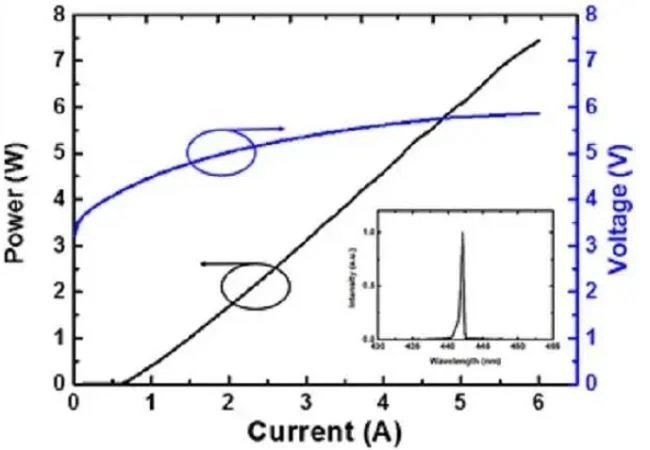
The current-optical power-voltage diagram of the blue laser developed by Liu Jianping's team at Suzhou Institute of Nanotechnology
We have noticed that the recent research on GaN-based lasers continues to heat up, and there are continuous reports on related developments. In March this year, the team of Kang Junyong and Li Jinchai of Xiamen University and San’an Optoelectronics achieved breakthrough results in a joint technology research project. The design and production of ultra-8-watt high-power InGaN blue lasers has reached international standards. The results were published in the journal Optics and Laser Technology
In August, the team of researcher Zhao Degang from the State Key Laboratory of Integrated Optoelectronics of the Institute of Semiconductors of the Chinese Academy of Sciences developed a gallium nitride (GaN)-based high-power blue laser with a continuous output power of up to 6 W at room temperature. The results were published in the Journal of Semiconductors (article information: doi: 10.1088/1674-4926/42/11/112801).
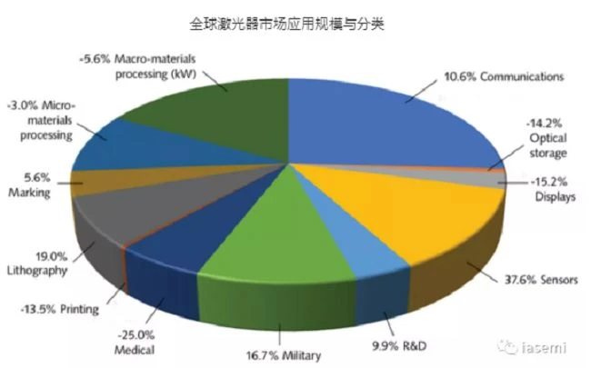
The research boom stems from the rapid and steady growth of the GaN laser market, which has begun to be widely used in many fields such as display, storage, military, medical, instrumentation, entertainment, lithography, and printing. However, GaN lasers are difficult to produce and have large technical barriers. The products have been controlled by several large international companies for a long time and are known as the jewel in the crown. The technical difficulties mainly include: high-quality substrate materials, high-quality epitaxial structures, high-quality ohmic contacts, and atomic crystal cleavage.
Global laser market application scale and classification
Taking high-quality substrate material as an example, the substrate is required to be a material with a low defect density. Compared with other GaN devices, GaN-based lasers have the most stringent requirements for crystal quality, because the current density of GaN lasers is one hundred or even thousand times that of ordinary devices. Therefore, if there are high-density defects of dislocations in the material, A leakage path will be formed, leading to rapid device failure.
The conventional method is to epitaxial the laser structure on the GaN single crystal substrate, and then prepare the semiconductor laser. At present, Sumitomo Electric, the world's top GaN monocrystalline substrate supplier, is also an important partner of Nichia, and has been strictly embargoed due to its important military use.
Fortunately, in recent years, major domestic substrate manufacturers represented by Suzhou Navitas and Dongguan Zhonggal have made rapid progress in the development of high-quality GaN single crystal substrates. The dislocation density of Navitas products has reached 104cm-2. , Reaching the world's advanced level, basically solving the dilemma of GaN laser substrate materials being "stuck" by foreign countries.
in conclusion
Nichia still controls the current high-power GaN laser market, while Sharp and Osram are the world's mainstream suppliers of small and medium-power GaN-based lasers. If my country wants to enter this market, it needs to increase investment in engineering and industrialization, and strive to overcome the problems and difficulties of industrialization, in order to completely break through the international monopoly and truly realize the localization of GaN-based lasers.


